AFM Resources

Anode oxidation of a Si substrate performed with a BudgetSensors ElectriTap300-G AFM probe on a JEOL JSPM-5200 AFM system
Scanned with a BudgetSensors Tap300E-G AFM probe, 4 micron scan size
Image courtesy of Takashi Sueyoshi, JEOL Ltd, Japan

Topography image of dried DNA
Scanned with a BudgetSensors Tap300Al-G AFM probe on an Asylum Cypher AFM system, 5 micron scan size
Image courtesy of Scott MacLaren, University of Illinois at Urbana-Champaign, USA

The BudgetSensors logo imprinted by scratch lithography on a flame annealed polycarbonate surface with a BudgetSensors Tap300Al-G AFM probe and an Asylum MFP 3D AFM system
Scanned with a BudgetSensors Tap300Al-G AFM probe on an Asylum MFP 3D AFM system, 20 micron scan size
Image courtesy of Scott MacLaren, University of Illinois at Urbana-Champaign, USA

Bismuth iron oxide (BFO) thin film on lanthanum aluminate (LAO)
Scanned with a BudgetSensors Tap300Al-G AFM probe on an Asylum Cypher AFM system, 20 micron scan size
Image courtesy of Scott MacLaren, University of Illinois at Urbana-Champaign, USA

Scanned with a BudgetSensors Tap300Al-G AFM probe on an Asylum Cypher AFM system, 4 micron scan size
Image courtesy of Scott MacLaren, University of Illinois at Urbana-Champaign, USA

Scanned with a BudgetSensors Tap300Al-G AFM probe and an Asylum MFP 3D AFM system, 2 micron scan size
Image courtesy of Scott MacLaren, University of Illinois at Urbana-Champaign, USA

Compressed silicon nanoribbons on a flexible PDMS substrate
Scanned with a BudgetSensors Tap300Al-G AFM probe on an Asylum MFP-3D AFM system, 90 micron scan size
Image courtesy of Scott MacLaren, University of Illinois at Urbana-Champaign, USA

Magnetic field MFM image of a zip disk
Scanned with a BudgetSensors Multi75M-G AFM probe on an Asylum MFP-3D AFM system, 75 micron scan size
Image courtesy of Scott MacLaren, University of Illinois at Urbana-Champaign, USA

A superconducting quantum photon detecting device
Scanned with a BudgetSensors Tap300Al-G AFM probe on an Asylum MFP-3D AFM system, 25 micron scan size
Image courtesy of Scott MacLaren, University of Illinois at Urbana-Champaign, USA

Mouse skeletal muscle fiber
Scanned with a BudgetSensors Tap300Al-G AFM probe on an Asylum MFP-3D AFM system, 20 micron scan size
Image courtesy of Scott MacLaren, University of Illinois at Urbana-Champaign, USA

A screw dislocation in a polymer surface
Scanned with a BudgetSensors Tap300Al-G AFM probe on an Asylum MFP-3D AFM system, 3 micron scan size
Image courtesy of Scott MacLaren, University of Illinois at Urbana-Champaign, USA

A crack in a nitride thin film
Scanned with a BudgetSensors Tap300Al-G AFM probe on an Asylum Cypher AFM system, 2 micron scan size
Image courtesy of Scott MacLaren, University of Illinois at Urbana-Champaign, USA

A gypsum crystal etched with water
Scanned with a BudgetSensors Tap300Al-G AFM probe on an Asylum Cypher AFM system, 3 micron scan size
Image courtesy of Scott MacLaren, University of Illinois at Urbana-Champaign, USA

Carbon nanotubes and bundles on quartz atomic steps
Scanned with a BudgetSensors Tap300Al-G AFM probe on an Asylum Cypher AFM system, 3 micron scan size
Image courtesy of Scott MacLaren, University of Illinois at Urbana-Champaign, USA

Topography image of the wing of a moth. The nanostructure makes the wing highly hydrophobic and it's directional - water droplets will only flow away from the body off the ends of the wing, keeping the body dry.
Scanned with a BudgetSensors Tap300Al-G AFM probe on an Asylum Research MFP-3D AFM system, 20 micron scan size
Image courtesy of Scott MacLaren, University of Illinois at Urbana-Champaign, USA

Single wall carbon nanotubes transferred to an elastic PDMS substrate, then laterally compressed, causing the nanotubes to buckle into waves
Scanned with a BudgetSensors Tap300Al-G AFM probe, 10 micron scan size
Image courtesy of Scott MacLaren, University of Illinois at Urbana-Champaign, USA

A thin strip of single layer graphene atop a ridged PDMS polymer substrate
Scanned with a BudgetSensors AIOAl AFM probe, Soft tapping mode cantilever (C), 10 micron scan size
Image courtesy of Scott MacLaren, University of Illinois at Urbana-Champaign, USA

Phase image of a SEBS block copolymer, topography rendered in 3D, overlaid with the color data from the phase image
Scanned with a BudgetSensors Tap300Al-G AFM probe, 4 micron scan size
Image courtesy of Scott MacLaren, University of Illinois at Urbana-Champaign, USA

Thin film of Zein protein with cholesterol
Scanned with a BudgetSensors Tap300Al-G AFM probe, 15 micron scan size
Image courtesy of Scott MacLaren, University of Illinois at Urbana-Champaign, USA

Atomic steps on a palladium surface
Scanned with a BudgetSensors Tap300Al-G AFM probe, 8 micron scan size
Image courtesy of Scott MacLaren, University of Illinois at Urbana-Champaign, USA

The curved surface of a human hair
Scanned with a BudgetSensors Tap300Al-G AFM probe, 35 micron scan size
Image courtesy of Scott MacLaren, University of Illinois at Urbana-Champaign, USA

The surface of an ant's abdominal plating
Scanned with a BudgetSensors Tap300Al-G AFM probe, 90 micron scan size
Image courtesy of Scott MacLaren, University of Illinois at Urbana-Champaign, USA

Strontium titanium oxide (SrTiO3) surface with 4 Angstrom steps
Scanned with a BudgetSensors Tap300Al-G AFM probe, 2 micron scan size
Image courtesy of Scott MacLaren, University of Illinois at Urbana-Champaign, USA

Dendritic growth of platinum nanoclusters
Scanned with a BudgetSensors Tap300Al-G AFM probe, 7 micron scan size
Image courtesy of Scott MacLaren, University of Illinois at Urbana-Champaign, USA

Hexagonal DNA nanostructure
Scanned with a BudgetSensors Tap300Al-G AFM probe, 600 nanometer scan size
Image courtesy of Scott MacLaren, University of Illinois at Urbana-Champaign, USA

Silicon surface impacted with molten copper droplet from the exhaust of a spacecraft ion thruster
Scanned with a BudgetSensors Tap300Al-G AFM probe, 25 micron scan size
Image courtesy of Scott MacLaren, University of Illinois at Urbana-Champaign, USA

Information on compact discs (CDs) is stored by a binary pattern of real physical holes in the plastic surface just below the reflective aluminum foil. During recording (or 'burning') a CD these holes are literally burned in the plastic by the laser in the CD/DVD players in our PCs and laptops.
Scanned with a BudgetSensors Tap300-G AFM probe, 25 micron scan size
Image courtesy of Dr. Yordan Stefanov ISB, Bulgaria

Crater in a sapphire substrate hit with a femtosecond laser pulse, followed by annealing to develop the step structure. The top surface is covered with single atomic steps (3Å).
Scanned with a BudgetSensors Tap300Al-G AFM probe, 20 micron scan size
Image courtesy of Scott MacLaren, University of Illinois at Urbana-Champaign, USA

An extremely thin (30 nm) free standing silicon nitride membrane with nickel nanoparticles, following heating with a short laser pulse. The nanoparticles react with the substrate, and the induced stress in the film creates large ripples in the membrane surface.
Scanned with a BudgetSensors Tap300Al-G AFM probe, 90 micron scan size
Image courtesy of Scott MacLaren, University of Illinois at Urbana-Champaign, USA

Finely detailed surface of biaxially-oriented polypropylene (BOPP)
Scanned with a BudgetSensors Tap300Al-G AFM probe, 3 micron scan size
Image courtesy of Scott MacLaren, University of Illinois at Urbana-Champaign, USA

Magnesium oxide (MgO) crystal, carved in a Focused Ion Beam (FIB) system. The top, unaltered surface shows single and double atomic steps.
Scanned with a BudgetSensors Tap300Al-G AFM probe, 20 micron scan size
Image courtesy of Scott MacLaren, University of Illinois at Urbana-Champaign, USA
Crystallization of poly(benzyl-beta-L-glutamate) on glass
Scanned with a BudgetSensors Tap300Al-G AFM probe, 30 micron scan size
Image courtesy of Scott MacLaren, University of Illinois at Urbana-Champaign, USA

Contaminants on the surface prior to sputtering give rise to classic sputter cone formation
Scanned with a BudgetSensors Tap300Al-G AFM probe, 1.5 micron scan size
Image courtesy of Scott MacLaren, University of Illinois at Urbana-Champaign, USA

Sapphire crystal following annealing at 1400°C, leaving a clean surface with atomic steps and occasional defects. The steps are approximately 3Å tall.
Scanned with a BudgetSensors Tap300Al-G AFM probe, 12 micron scan size
Image courtesy of Scott MacLaren, University of Illinois at Urbana-Champaign, USA

Xanthomonas campestris bacteria in potato agar
Scanned with a BudgetSensors Multi75Al-G AFM probe in light tapping mode, 10 micron scan size
Image courtesy of Dr. Yordan Stefanov, Innovative Solutions Bulgaria

Chocolate is a complex material consisting primarily of a finely crystallized continuous fatty lipid matrix (cocoa butter) in which cocoa powder and sugar particles are dispersed. With time, the lipid crystals tend to merge to form larger crystals on a micron scale, significantly effecting the texture and taste of the chocolate. These images are of an aged commercial dark chocolate sample. The topography of the surface is rendered in 3D, while the coloring is an overlay of the phase image, which highlights the compositional differences (darker patches being the growing cocoa butter crystals).
Scanned with a BudgetSensors Tap300Al-G AFM probe, 15 micron scan size
Image courtesy of Scott MacLaren, University of Illinois at Urbana-Champaign, USA

E-coli bacterium with flagellum
Scanned with a BudgetSensors Tap300Al-G AFM probe, 6 micron scan size
Image courtesy of Scott MacLaren, University of Illinois at Urbana-Champaign, USA

Highly Oriented Pyrolytic Graphite (HOPG) sample
Scanned with a BudgetSensors Tap300Al-G AFM probe., 1024 nanometer scan size
Image courtesy of Albert Lin, Angsnanotek Co., Ltd., Taiwan

Phase image of a styrene-ethylene-butylene-styrene (SEBS) triblock copolymer
Scanned with a BudgetSensors Tap300Al-G AFM probe, 3 micron scan size
Image courtesy of Scott MacLaren, University of Illinois at Urbana-Champaign, USA

The porous surface of anodized aluminum
Scanned with a BudgetSensors Tap300Al-G AFM probe, 3 micron scan size
Image courtesy of Scott MacLaren, University of Illinois at Urbana-Champaign, USA

Zinc oxide nanoparticles (20~50nm)
Scanned with a BudgetSensors Tap300Al-G AFM probe, 256 to 1024 nanometer scan size
Image courtesy of Albert Lin, Angsnanotek Co., Ltd., Taiwan

Atomic steps on sputtered palladium
Scanned with a BudgetSensors Tap300Al-G AFM probe, 2.5 micron scan size
Image courtesy of Scott MacLaren, University of Illinois at Urbana-Champaign, USA

Carbon nanotube (CNT), 2nm
Scanned with a BudgetSensors Tap300Al-G AFM probe, 2048, 1024, 512 and 256 nanometer scan sizes, respectively
Image courtesy of Albert Lin, Angsnanotek Co., Ltd., Taiwan

Amyloid fibrils (4~8nm)
Scanned with a BudgetSensors Tap300Al-G AFM probe, 256 to 1024 nanometer scan size
Image courtesy of Albert Lin, Angsnanotek Co., Ltd., Taiwan

Screw dislocation in poly-oxy-methylene (POM)
Scanned with a BudgetSensors Tap300Al-G AFM probe, 3 micron scan size
Image courtesy of Jeff Kalish, University of Illinois at Urbana-Champaign, USA

Surafece topography (left) and magnetic field (right) images of the surface of a magnetic ZIP disk
Scanned with a BudgetSensors Multi75M-G AFM probe, 60 micron scan size
Image courtesy of Scott MacLaren, University of Illinois at Urbana-Champaign, USA

Topographic image (left) and Magnetic Force Microscopy (MFM) phase image (right) of a HDD platter surface. The high and low areas on the magnetic scan are regions with different orientation of the magnetic dipoles that store binary 1s and 0s
Scanned with a BudgetSensors Multi75M-G AFM probe in Magnetic Force Microscopy mode, 5 micron scan size
Image courtesy of Dr. Yordan Stefanov, Innovative Solutions Bulgaria

Electrostatic Force Microscopy (EFM) test sample with differently biased metal lines. The topographic data (first image) shows two metal lines and the electrostatic force data helps distinguish between the biased line (left, 2 Volts) and the grounded one (right).
Scanned with a BudgetSensors Multi75E-G AFM probe in Electrostatic Force Microscopy mode, 7 micron scan size
Image courtesy of Dr. Yordan Stefanov, Innovative Solutions Bulgaria

Topography (left) and 3D topography (right) images of nanoparticles
Scanned with a BudgetSensors Tap300Al-G AFM probe, 1024 nanometer scan size
Image courtesy of Albert Lin Angsnanotek Co., Ltd., Taiwan

Scanned with a BudgetSensors Tap300Al-G AFM probe, 5000, 2000, 1024 and 512 nanometer scan size, respectively
Image courtesy of Albert Lin, Angsnanotek Co., Ltd., Taiwan

Partially mixed and partially cured two component epoxy. The phase image data is overlaid on the 3D topography.
Scanned with a BudgetSensors Tap190Al-G AFM probe, 5 micron scan size
Image courtesy of Dr. Yordan Stefanov, Innovative Solutions Bulgaria

Imprints of different porphyrin aggregates in polystyrene
Scanned with a BudgetSensors Tap300Al-G AFM probe, 2.5 micron scan size
Image courtesy of Walter Smith, Haverford College, Haverford, USA

ZnO particles (<10nm)
Scanned with a BudgetSensors Tap300Al-G AFM probe, 1024, 512, 256 and 256 nanometer scan size, respectively
Image courtesy of Albert Lin, Angsnanotek Co., Ltd., Taiwan

Topography (left), PFM amplitude (center) and PFM phase (right) images of polycrystalline Pb(Zr0.3Ti0.7)O3 thin film
Scanned with a BudgetSensors Multi75E-G AFM probe, 1 micron scan size
Image courtesy of Prof. Yunseok Kim, Sungkyunkwan University, South Korea

Topography and 3D topography images of polycrystalline SrTiO3 single crystal substrate
Scanned with a BudgetSensors ContAl-G AFM probe in contact mode, 5 micron scan size
Image courtesy of Prof. Yunseok Kim, Sungkyunkwan University, South Korea

Kelvin Probe Measurement on graphene exfoliated on strontium titanate (SrTiO3) obtained in non-contact AFM mode using a frequency shift of -5 Hz. The graphene was irradiated with xenon 23+ ions under grazing incidence of 6°. On monolayer the impact of the ions lead to characteristic folding. In Bias-Image the exposed underlying substrate in this area can be clearly seen. Also, the monolayer shows lower surface potential difference to SrTiO3 than few monolayers.
Scanned with a BudgetSensors Tap300E-G AFM probe on a RHK Technology SPM 1000 Control System
Image courtesy of Benedict Kleine Bussmann, Oliver Ochedowski, Marika Schleberger AG Schleberger, University Duisburg-Essen

Scanned with a BudgetSensors Tap300Al-G AFM probe, 2 micron scan size
Image courtesy of Scott MacLaren, University of Illinois at Urbana-Champaign, USA

Carbon nanotubes and bundles emerging from line of catalyst particles
Scanned with a BudgetSensors Tap300Al-G AFM Probe, 5 micron scan size
Image courtesy of Scott MacLaren, University of Illinois at Urbana-Champaign, USA

Fast dried white glue.
Scanned with a BudgetSensors Tap300Al-G AFM probe, amplitude image, 10 micron scan size
Image courtesy of Scott MacLaren, University of Illinois at Urbana-Champaign, USA

Scanned with a BudgetSensors Tap300Al-G AFM Probe, 10 micron scan size
Image courtesy of Scott MacLaren, University of Illinois at Urbana-Champaign, USA

Magnetic field image of high capacity (500 GB) hard disk
Scanned with a BudgetSensors Multi75M-G AFM Probe, 10 micron scan size
Image courtesy of Scott MacLaren, University of Illinois at Urbana-Champaign, USA

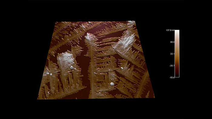
Dendritic growth of HDI polymer
Scanned with a BudgetSensors Tap300Al-G AFM Probe, 20 micron scan size
Image courtesy of Scott MacLaren, University of Illinois at Urbana-Champaign, USA

Scanned with a BudgetSensors Tap300Al-G AFM probe, 10 micron scan size
Image courtesy of Scott MacLaren, University of Illinois at Urbana-Champaign, USA

Scanned with a BudgetSensors Tap300Al-G AFM probe, 3 micron scan size
Image courtesy of Scott MacLaren, University of Illinois at Urbana-Champaign, USA

Scanned with a BudgetSensors Tap300Al-G AFM probe, 30 micron scan size
Image courtesy of Scott MacLaren, University of Illinois at Urbana-Champaign, USA

Scanned with a BudgetSensors Tap300Al-G AFM probe, 90 micron scan size
Image courtesy of Scott MacLaren, University of Illinois at Urbana-Champaign, USA

Scanned with a BudgetSensors Tap300Al-G AFM probe, 10 micron scan size
Image courtesy of Scott MacLaren, University of Illinois at Urbana-Champaign, USA

Ruptured gold palladium thin film
Scanned with a BudgetSensors Tap300Al-G AFM probe, 5 micron scan size
Image courtesy of Scott MacLaren, University of Illinois at Urbana-Champaign, USA

Two dimensional plastic optical grating
Scanned with a BudgetSensors Tap300Al-G AFM probe, 30 micron scan size
Image courtesy of Scott MacLaren, University of Illinois at Urbana-Champaign, USA

Water etched gypsum crystal
Scanned with a BudgetSensors Tap300Al-G AFM probe, 1 micron scan size
Image courtesy of Scott MacLaren, University of Illinois at Urbana-Champaign, USA

A scan of synthetic opal
Scanned with a BudgetSensors Tap300Al-G AFM probe, 9 micron scan size
Image courtesy of Scott MacLaren, University of Illinois at Urbana-Champaign, USA

Scanned with a BudgetSensors Tap300Al-G AFM probe, 30 micron scan size
Image courtesy of Scott MacLaren, University of Illinois at Urbana-Champaign, USA

Polymer blend of polystyrene and polycaprolactone
Scanned with a BudgetSensors Tap300Al-G AFM probe, 10 micron scan size
Image courtesy of Scott MacLaren, University of Illinois at Urbana-Champaign, USA

Scanned with a BudgetSensors Tap300Al-G AFM probe, 12 micron scan size
Image courtesy of Scott MacLaren, University of Illinois at Urbana-Champaign, USA

Scanned with a BudgetSensors Tap300Al-G AFM probe, 80 micron scan size
Image courtesy of Scott MacLaren, University of Illinois at Urbana-Champaign, USA

SRAM memory device
Scanned with a BudgetSensors Tap300Al-G AFM probe, 70 micron scan size
Image courtesy of Scott MacLaren, University of Illinois at Urbana-Champaign, USA

Scanned with a BudgetSensors Tap300Al-G AFM probe, 90 micron scan size
Image courtesy of Scott MacLaren, University of Illinois at Urbana-Champaign, USA

Scanned with a BudgetSensors Tap300Al-G AFM probe, 90 micron scan size
Image courtesy of Scott MacLaren, University of Illinois at Urbana-Champaign, USA

Scanned with a BudgetSensors Tap300Al-G AFM probe, 20 micron scan size
Image courtesy of Scott MacLaren, University of Illinois at Urbana-Champaign, USA

Scanned with a BudgetSensors Tap300Al-G AFM probes, 2500, 1000 and 500 nanometer scan size, respectively
Image courtesy of Albert Lin, Angsnanotek Co., Ltd., Taiwan

The first virus ever discovered and one of the most thoroughly researched, the tobacco mosaic virus (TMV) attacks various plant species and especially tobacco. The name of the rod-shaped RNA virus comes from the mosaic-like symptoms it causes.
Scanned with a BudgetSensors Tap150Al-G AFM probe, 5 micron scan size,
Image courtesy of Dr. Yordan Stefanov, Innovative Solutions Bulgaria

A definite favorite of AFM researchers worldwide (or at least of the one who produced this image), Lindt’s 99% cocoa Excellence bar has very intense cocoa taste. The topography image of a bar’s back surface is rendered in 3D and overlaid with the phase image. The false-color yellowish spots are regions of growing cocoa butter crystals.
Scanned with a BudgetSensors Tap150Al-G AFM probe, 15 micron scan size
Image courtesy of Dr. Yordan Stefanov, Innovative Solutions Bulgaria; inspired by Scott MacLaren, UIUC, USA

BudgetSensors CS-20NG calibration nanogrid. Structure-wise, the nanogrid differs from our microgrids by the additional array of circular holes with a 500 nanometer pitch. The images shows the transition between the microarrays and the nanoarray.
Scanned with a BudgetSensors AIOAl AFM probe, cantilever B (Multi75-like) in contact mode, 20 micron scan size
Image courtesy of Dr. Yordan Stefanov, Innovative Solutions Bulgaria

The TipCheck is our AFM probe tip evaluation sample. The sharp pyramidal structures allow reverse imaging of the tip apex.
Scanned with a BudgetSensors Tap300Al-G AFM probe, 1 micron scan size
Image courtesy of Dr. Yordan Stefanov, Innovative Solutions Bulgaria

Topography image of the central area of BudgetSensors height calibration standard HS-100MG with 100 nm nominal step height. The HS-100MG can also be used for X-Y calibration of large area scanners. The array design makes it possible to calibrate your AFM system without the need to rotate and realign the sample in-between X and Y axis calibration.
Scanned with a BudgetSensors Tap300Al-G AFM probe, 25 micron scan size
Image courtesy of Dr. Yordan Stefanov, Innovative Solutions Bulgaria

Tapping mode topography (left) and electrostatic force microscopy overlaid on topography (right) images of metal lines on an insulating substrate. EFM helps distinguish the two lines biased at 3V from the grounded one in the middle.
Scanned with a BudgetSensors Multi75E-G AFM probe, 10 micron scan size
Image courtesy of Dr. Yordan Stefanov, Innovative Solutions Bulgaria

This is a topography image of a holographic, UV optimized, blazed diffraction grating with 2400 lines/mm. It is a good graphic illustration of how much further at the nanoscale Atomic Force Microscopy allows us to ‘see’ beyond what any optical device could. The ridges diffract visible and near-UV light. To light these ridges are perfectly flat. The AFM using a sharp BudgetSensors tip shows us that their surface is actually quite rough.
Scanned with a BudgetSensors SiNi AFM probe, long cantilever in contact mode, 3 micron scan size
Image courtesy of Dr. Yordan Stefanov, Innovative Solutions Bulgaria

Tapping mode topography (left) and magnetic force microscopy overlaid on topography (right) images of the surface of a harddrive platter. MFM reveals the hidden bits of information stored by magnetizing small regions of a ferromagnetic film.
Scanned with a BudgetSensors Multi75M-G AFM probe, 10 micron scan size
Image courtesy of Dr. Yordan Stefanov, Innovative Solutions Bulgaria

For accurate imaging of small features the AFM tip radius of curvature must be much smaller than the typical feature size. If, on the contrary, the tip is much larger than the features, the result of the measurement is an image of the tip itself! On the left is a tapping mode scan with a brand new sharp probe that reveals nicely the pyramidal structures on our TipCheck. On the right is a scan of the same TipCheck using a damaged tip. One can see clearly the triangular crosssection of the tip pyramid broken-off by improper probe handling.
Scanned with a BudgetSensors Tap300Al-G AFM probe, 1 micron scan size
Image courtesy of Dr. Yordan Stefanov, Innovative Solutions Bulgaria

Did you know that collagen is the most abundant protein in our bodies making up around 30% of total protein content?
Scanned with a BudgetSensors Tap300Al-G AFM probe, 40 micron scan size
Image courtesy of Scott MacLaren, University of Illinois at Urbana-Champaign, USA

Precious opals are composed of closely packed silica spheres with sizes of several hundred nanometers. The beautiful colors of opals are caused by light diffraction and interference. This 90 micron AFM scan shows an opal surface with two transitions between neighboring planes of nanospheres.
Scanned with a BudgetSensors Tap300Al-G AFM probe, 90 micron scan size
Image courtesy of Scott MacLaren, University of Illinois at Urbana-Champaign, USA

Large scale structure of a desiccated compound butterfly eye (left) and fine nanostructure completely covering the facets (right)
Scanned with a BudgetSensors Tap300Al-G AFM probe, 90 and 4 micron scan size, respectively
Image courtesy of Scott MacLaren, University of Illinois at Urbana-Champaign, USA

A contact mode topography image rendered in 3D and overlaid with the Lateral Force Microscopy image shows nicely the scales’ morphology as well as some hairspray droplets on a human hair.
Scanned with a BudgetSensors ContAl-G AFM probe, 40 micron scan size
Image courtesy of Dr. Yordan Stefanov, Innovative Solutions Bulgaria

Information is stored on CDs by real physical holes in the plastic surface below the reflective aluminum foil. The laser holes on CD-Rs and DVD-Rs we 'burn' at home probably look a bit different from the molded ones on mastered CDs.
Scanned with a BudgetSensors Tap190Al-G AFM probe, 20, 10 and 2.5 micron scan size
Image courtesy of Dr. Yordan Stefanov, Innovative Solutions Bulgaria

Topography of the transition area between the shiny polished side of the blade and its sharpened cutting edge
Scanned with a BudgetSensors AIOAl AFM probe, cantilever C (Tap150-like), 35 micron scan size
Image courtesy of Dr. Yordan Stefanov, Innovative Solutions Bulgaria

Topography scan of bacteria and negative imprints thereof in dried potato agar
Scanned with a BudgetSensors SiNi AFM probe, long cantilever, 10 micron scan size
Image courtesy of Dr. Yordan Stefanov, Innovative Solutions Bulgaria

The XC bacteria cause a number of diseases in plants. They are also used in the food industry to create the food additive xantham gum, a common thickening agent.
Scanned with a BudgetSensors Multi75Al-G AFM probe in light tapping mode, 10, 5 and 0.5 micron scan size. respectively
Image courtesy of Dr. Yordan Stefanov, Innovative Solutions Bulgaria

Topography image of human platelet acquired at room temperature
Scanned with a BudgetSensors ContAl-G AFM probe, 6 micron scan size
Image courtesy of Dr. Tonya Andreeva, Institute of Biophysics and Biomedical Engineering, BAS

Topography of CdSe thin film. Estimated mean nanocrystalline size is less than 10nm.
Scanned with a BudgetSensors Tap150Al-G AFM probe on a Bruker MultiMove V AFM system. 50 nanometer scan size
Image courtesy of Dr. Irina Bineva, Institute of Solid State Physics, BAS

Cd enriched areas in Zn0.4Cd0.6Se, topography and phase image. In order to obtain simultaneously good contrast in the phase image without distortion in the height image, due to surface damage, interleave mode with light tapping conditions for the height scan, and hard tapping for the phase image was used, repectively.
Scanned with a BudgetSensors Tap150Al-G AFM probe on a Bruker MultiMode V AFM system. 500 nanometer scan size
Image courtesy of Dr. Irina Bineva, Institute of Solid State Physics, BAS

Zn0.5Cd0.5Se thin film. Z axis max value is 16.6 nm.
Scanned with a BudgetSensors Tap150Al-G AFM probe on a Bruker MultiMode V AFM system, 1 micron scan size
Image courtesy of Dr. Irina Bineva, Institute of Solid State Physics, BAS

Scanned with a BudgetSensors Tap300E-G AFM probe, 8 micron scan size
Image courtesy of Steve Liu, Dual Signal Tech Corp.

The blend of two biopolymers with compatibilizer
Scanned with a BudgetSensors Tap300Al-G AFM probe, 2 micron scan size
Image courtesy of Nagoya Municipal Industrial Research Institute, Japan

Scanned with a BudgetSensors Tap300Al-G AFM probe, 55 micron scan size
Image courtesy of Scott MacLaren, University of Illinois at Urbana-Champaign, USA